The development of electronic devices has been rapidly progressing, with a focus on creating smaller and more efficient devices. Two-dimensional (2D) semiconducting materials have emerged as a promising avenue for achieving this goal. These materials offer significant advantages over their traditional bulky counterparts, such as retaining carrier mobility even with reduced thickness. However, the application of 2D semiconductors in monolayer transistors, which are essential components of electronic devices, has been limited. Existing monolayer transistors have mostly been created using well-known materials like graphene and tungsten diselenide. Researchers from Hunan University, the Chinese Academy of Sciences, and Wuhan University sought to expand the possibilities of monolayer transistors by utilizing alternative 2D semiconducting materials such as black phosphorus (BP) and germanium arsenide (GeAs). Their findings were published in the journal Nature Electronics.
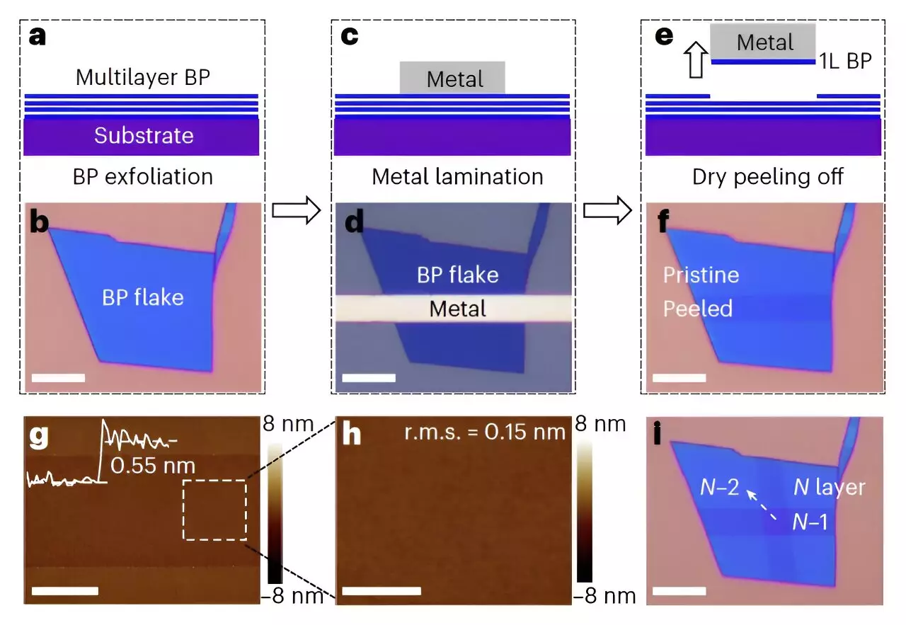
Creating monolayer transistors using 2D semiconductors presents multiple challenges. Some materials are difficult to uniformly scale down without compromising their inherent properties. Moreover, forming robust electrical contacts with delicate 2D materials can be problematic. To address these issues, the researchers, led by Wangying Li and Quanyang Tao, proposed a van der Waals (vdW) peeling technique. This technique involves laminating flat metals onto multi-layer 2D channels, allowing the removal of the top semiconducting layer by peeling off the metal. The team successfully utilized this technique to fabricate monolayer black phosphorus and germanium arsenide transistors with 3D raised contacts.
The vdW peeling technique developed by Li, Tao, and their colleagues offers an innovative approach to fabricate monolayer transistors using alternative 2D semiconductors. By gradually reducing the channel region of a multilayer black phosphorus transistor through layer-by-layer mechanical peeling, the delicate lattice of the material is preserved. Simultaneously, the thickness of the contact region, which is crucial for transistor functionality, remains unaffected. This method enables the researchers to thin down the channel part while maintaining the required thickness in the contact region.
During their study, the team successfully applied the vdW peeling technique to create homo-junctions and homo-superlattices utilizing various 2D semiconductors, including black phosphorus, germanium arsenide, indium selenide (InSe), and gallium selenide (GaSe). The researchers observed that their proposed technique allowed for the careful adjustment of the channel thickness while preserving the electrical properties of the transistors. Interestingly, they discovered that as the body thickness of black phosphorus decreased, the carrier mobility dropped significantly, behaving more like a conventional bulk semiconductor rather than a pure vdW semiconductor.
The recent study conducted by Li, Tao, and their colleagues demonstrated the potential of the vdW peeling technique in developing monolayer transistors with 3D-raised contacts based on black phosphorus and germanium arsenide. This innovative method could open new possibilities for creating thinner and more scalable transistors using unconventional 2D semiconductors. Notably, the researchers also noted that their work could have implications for other unstable monolayer materials beyond 2D semiconductors, such as organic monolayers and perovskite monolayers. These materials, previously considered non-conductive or possessing poor intrinsic properties, may benefit from improved metal-monolayer contact enabled by the peeling technique.
The advancement of 2D semiconductors in monolayer transistors represents a significant breakthrough in the field of electronics. By overcoming the challenges associated with the fabrication of these transistors using alternative 2D semiconducting materials, Li, Tao, and their colleagues have demonstrated a new approach to create thinner and more efficient electronic devices. The vdW peeling technique shows promise in expanding the range of materials suitable for monolayer transistors, potentially revolutionizing the field and paving the way for further advancements in wearable technology and smaller electronics.
Leave a Reply