The field of photonic integrated circuits has gained significant attention due to its potential applications in data centers, artificial intelligence, quantum computing, and more. The use of photons instead of electrons in electronic circuits offers improved performance and cost-effectiveness. However, the challenge lies in accurately mapping the internal light motion of photonic chips, which are characterized by their small dimensions and fabrication flaws. Addressing this challenge, researchers from Technion’s Andrew and Erna Viterbi Faculty of Electrical and Computer Engineering have developed a novel technique for advanced light imaging in photonic circuits on chips.
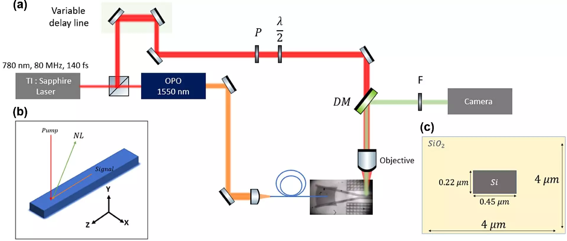
Led by Professor Guy Bartal and doctoral student Matan Iluz, the research team utilized the optical characteristics of silicon to map the propagation of light without any invasive action that could alter the chip. By mapping the electric field of the light waves and identifying the elements affecting its movement, such as waveguides and beam splitters, the researchers were able to generate real-time images and video recordings of the light inside the photonic chip. This non-destructive approach provides valuable insights without compromising the chip’s integrity or losing any data.
The development of this advanced imaging technique is poised to revolutionize the design, production, and optimization processes of photonic chips. The ability to visualize the internal light behavior in real-time enables engineers to better understand the impact of fabrication flaws and inaccuracies, ultimately leading to improved chip performance. This breakthrough has implications across a wide range of fields, including telecommunications, high-performance computing, machine learning, measuring distances, medical imaging, sensing, and quantum computing.
With the precise mapping of the light waves’ electric field, researchers can identify areas within the photonic chip that may impede optimal performance. By determining the factors influencing the light’s movement, engineers can address design flaws and refine the structures responsible for light guidance. Furthermore, the ability to visualize the light propagation process in real-time allows for the identification of inefficiencies and the subsequent optimization of the chip’s design. This advanced imaging technique empowers engineers to fine-tune the performance of photonic chips, leading to enhanced overall efficiency and cost-effectiveness.
The impact of advanced light imaging extends beyond the realm of photonic chips. In telecommunications, the ability to accurately map and visualize light propagation enables the development of faster and more reliable communication networks. In high-performance computing and machine learning, this technique facilitates the optimization of photonic circuits, offering increased computational power and energy efficiency. Additionally, in medical imaging, the real-time imaging of light inside the photonic chip can enhance the quality and accuracy of diagnostic procedures. The applications also extend to quantum computing, where precise light manipulation is crucial for the development of quantum algorithms and quantum information processing.
As the field of photonic integrated circuits continues to advance, the development of novel imaging techniques becomes increasingly important. The research conducted at Technion’s Andrew and Erna Viterbi Faculty of Electrical and Computer Engineering represents a significant step towards overcoming the challenges associated with accurate mapping of light propagation in photonic chips. By harnessing the optical characteristics of silicon, researchers have demonstrated the potential to improve chip design, production, and optimization processes across various industries. With further advancements and refinements, photonic integrated circuits have the potential to revolutionize numerous fields, paving the way for a more efficient and technologically advanced future.
Leave a Reply