In the realm of miniaturized optoelectronic devices, high gate capacitance is crucial for optimal performance while consuming less energy. This has led researchers to explore various approaches to enhance gate capacitance without compromising the thickness of gate insulators or dielectrics. One such method involves utilizing insulating materials with a high dielectric constant (κ), such as hafnium oxide (HfO2). However, integrating these materials with 2D semiconductors has proven to be a challenging task.
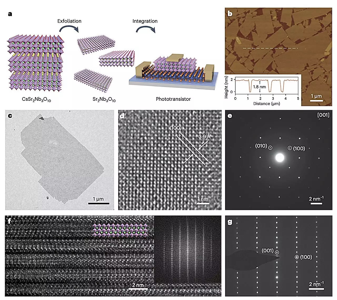
Researchers at Fudan University have recently made a groundbreaking discovery in this area by introducing a 2D perovskite oxide with a high dielectric constant that can be seamlessly integrated with different 2D channel materials. The perovskite oxide, Sr2Nb3O10, exhibits a high κ of 24.6 along with a moderate bandgap, making it an ideal candidate for a photoactive high-κ dielectric in phototransistors based on various 2D semiconducting materials.
To assess the potential of Sr2Nb3O10 in developing miniaturized optoelectronics, the researchers transferred the oxide onto different channel materials, including graphene, molybdenum disulfide, tungsten disulfide, and tungsten diselenide. The performance of transistors integrating these materials with Sr2Nb3O10 was evaluated, showing promising results with high on/off ratios, low subthreshold swing, and excellent photocurrent-to-dark-current ratios.
One of the key highlights of this study was the efficient gate control achieved through the interface established between the semiconductor and the high-κ dielectric. The researchers also demonstrated the capability of the phototransistors with the photoactive dielectric to offer UV-visible dual-band photodetection, distinguishing between UV and visible light illuminations at separate terminals.
The successful integration of Sr2Nb3O10 with various channel materials opens up new possibilities for the synthesis of additional 2D perovskite oxides that can be combined with existing semiconductors and channel materials. These advancements hold the promise of creating smaller, high-performing, and energy-efficient electronics and optoelectronics, paving the way for a new era in device design and technology.
The research conducted by Li, Liu, and their colleagues at Fudan University represents a significant step forward in the field of 2D superconducting materials for optoelectronic device development. Their innovative approach and experimental findings contribute valuable insights to the ongoing quest for more efficient, scalable, and high-performance electronic technologies.
Leave a Reply