In a recent study conducted by a research team in Japan, a major breakthrough has been achieved in the observation of magnetic fields at incredibly small scales. This study involved scientists from renowned institutions such as Hitachi, Ltd., Kyushu University, RIKEN, and HREM Research Inc. By utilizing Hitachi’s atomic-resolution holography electron microscope and implementing innovative image acquisition technology and defocus correction algorithms, the team was able to visualize the magnetic fields of individual atomic layers within a crystalline solid. This breakthrough has the potential to revolutionize the field of materials science and lead to significant advancements in various industries.
Understanding and observing magnetic fields at the atomic level is crucial for the development of high-performance materials with tailored characteristics. The orientation and strength of magnetic fields at the interface between different materials or atomic layers play a vital role in determining the properties of a crystalline material. These magnetic fields can often explain peculiar physical phenomena and help scientists unlock new possibilities in electronics, catalysis, transportation, and energy generation. Prior to this breakthrough, the observation of magnetic fields at atomic layers was limited to a resolution of around 0.67 nm. However, with the recent advancements, researchers have been able to push this limit even further.
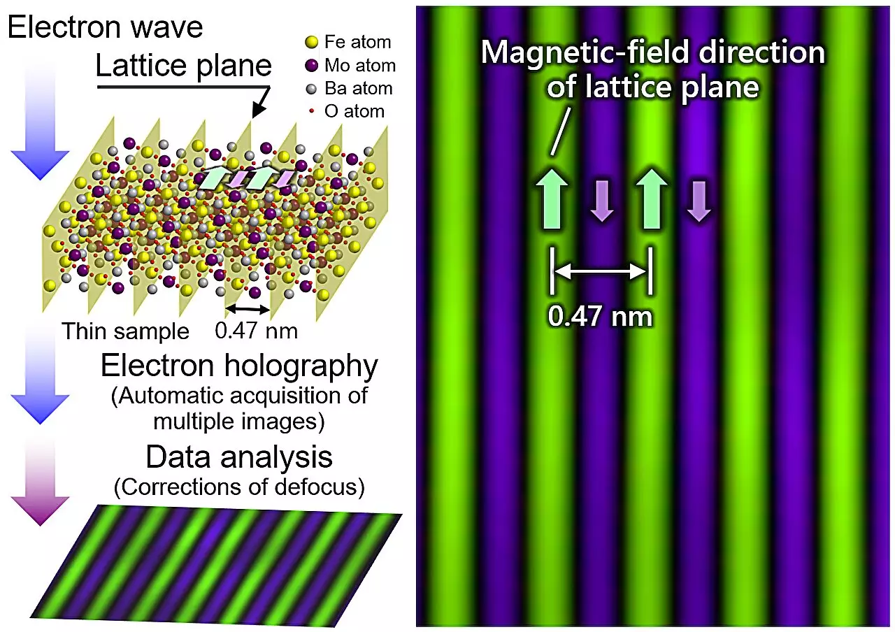
The research team addressed several key limitations in Hitachi’s holography electron microscope to achieve this groundbreaking result. They developed a system to automate the control and tuning of the device during data acquisition, significantly speeding up the imaging process. By performing specific averaging operations with the acquired images, they were able to minimize noise and obtain clearer images containing distinct electric field and magnetic field data. Additionally, the team implemented a technique to correct for minute defocusing, which caused aberrations in the images. This correction method involved analyzing reconstructed electron waves to eliminate residual aberrations and enhance the visibility of atoms with magnetic field data.
The researchers conducted electron holography measurements on samples of Ba2FeMoO6, a layered crystalline material with distinct magnetic fields in adjacent atomic layers. By comparing their experimental results with simulations, the team confirmed that they had achieved a record resolution of 0.47 nm in observing the magnetic fields of Ba2FeMoO6. This significant improvement opens up new possibilities for directly observing magnetic lattices in specific areas such as interfaces and grain boundaries in various materials and devices. Chief Researcher Toshiaki Tanigaki expressed optimism about the potential of this breakthrough to unveil veiled phenomena and advance scientific and technological discoveries.
The research team believes that their achievement in observing magnetic fields at such high resolution will have far-reaching implications for various fields, from fundamental physics to the development of next-generation devices. The atomic-resolution holography electron microscope developed by Hitachi is expected to be utilized by different parties to drive innovation across industries. This technological advancement could lead to the realization of a carbon-neutral society by facilitating the development of high-performance magnets and highly functional materials essential for decarbonization and energy-saving efforts. The team’s groundbreaking research marks a significant step towards solving complex scientific and technological challenges and lays the groundwork for future discoveries in the field of materials science.
Leave a Reply