Recent advancements in semiconductor research have taken a significant leap forward thanks to a team of researchers at UC Santa Barbara. They have managed to create the first-ever visual “movie” of electric charges as they traverse the boundary between two different semiconductor materials. By employing scanning ultrafast electron microscopy (SUEM), developed under the expertise of Bolin Liao, the group has successfully captured an elusive phenomenon that has been extensively theorized but practically elusive. This groundbreaking work, published in the *Proceedings of the National Academy of Sciences*, constitutes a pivotal moment in understanding semiconductor behavior, allowing for the potential recalibration of established theories.
Historically, the complex process of carrier movement within semiconductors has been relegated to the realm of indirect observations, primarily supported by theories laid out in textbooks. Liao, an associate professor of mechanical engineering, emphasizes the critical nature of direct visualizations, stating that such advancements can finally provide tangible insights to benchmark various semiconductor theories. In essence, witnessing the dynamics of charge carriers—the fundamental building blocks of semiconductor functionality—can reshape our understanding of their behavior as well as refine fabrication processes in technological applications.
To comprehend the significance of this research, one must grasp the role that photocarriers play in our energy landscape. When sunlight interacts with a semiconductor, it stimulates electrons to become energized, resulting in electric currents. In practice, however, these “hot carriers” tend to lose most of their energy in picoseconds—a timeframe that considerably hinders their immediate usability for applications like solar energy conversion. Thus, understanding these high-energy states is not just a matter of curiosity; it is vital for enhancing energy efficiency and device performance.
Additionally, the behavior of these hot carriers across a heterojunction, where two different semiconductor materials meet, becomes especially crucial. Semiconductor heterojunctions govern carrier movement and are foundational in various technologies, from photovoltaics to sensors and lasers. Therefore, discerning the interaction of charge movement in this nuanced environment presents significant implications for the engineering of more efficient devices.
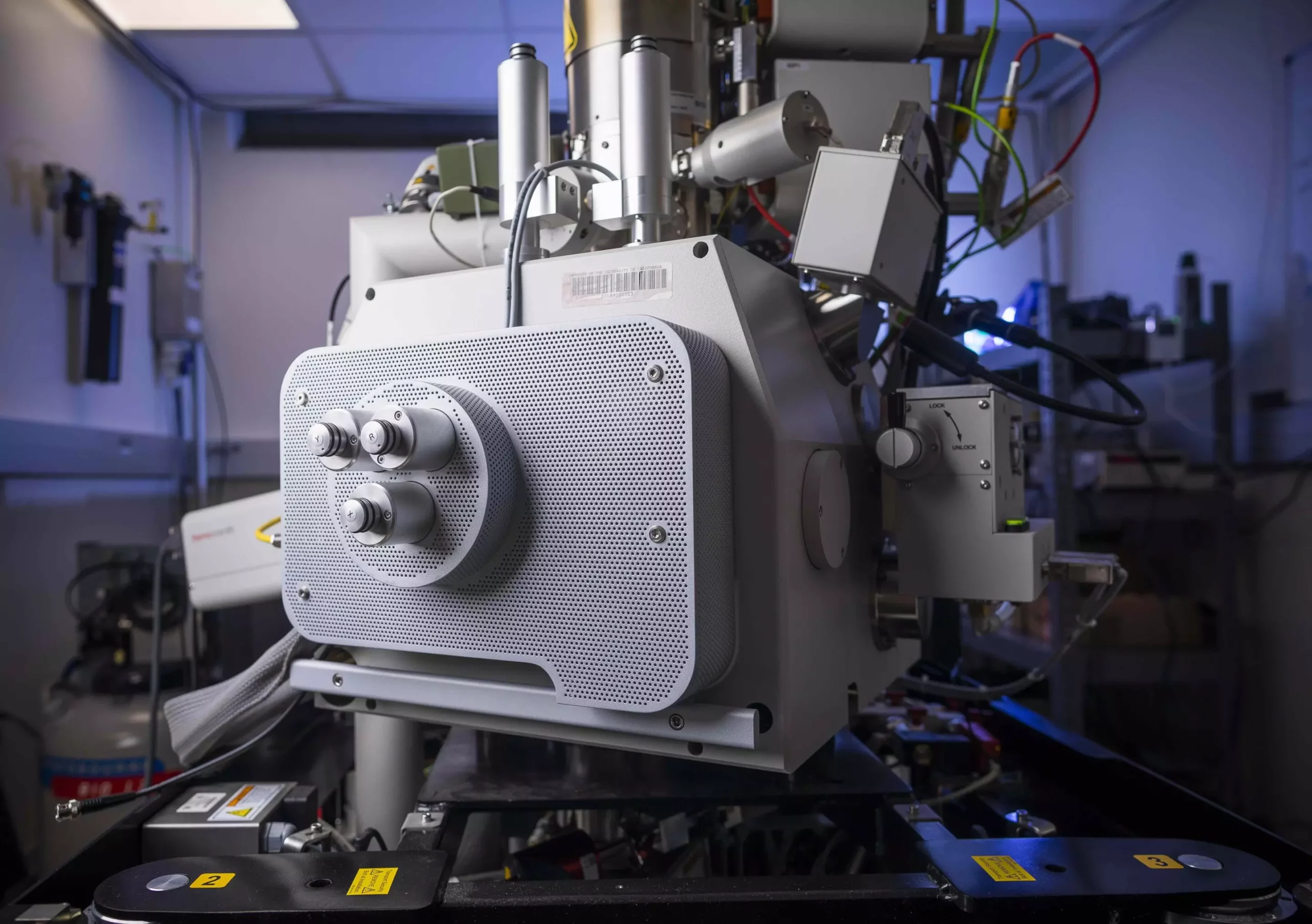
The team’s innovative SUEM technique relies on ultrafast laser pulses serving as a shutter within a picosecond-scale timeframe. This approach allows researchers to synchronize an electron beam with the transitions of hot photocarriers, providing a unique perspective on their movement. As Liao asserts, capturing events that unfold between the picosecond and nanosecond intervals requires an unprecedented precision in microscopy—a challenge that this research rose to meet.
Significantly, the results illustrated how charges behave differently depending on their location in relation to the semiconductor interface. Those excited in the uniform regions of silicon or germanium exhibit high velocities attributed to their elevated temperatures. Conversely, the charges pushed into the junction are subject to potential traps that considerably slow their mobility. This trapping phenomenon, while predictable through established semiconductor theory, has never been visualized directly until now—a remarkable indicator of the research’s success.
The implications of this research extending far beyond the academic realm are profound. For semiconductor device designers, understanding charge trapping within Si/Ge heterojunctions may spark a redesign of existing devices to mitigate performance losses. The visual evidence provided by the SUEM technique does not just serve as a confirmation of theoretical predictions; it concretely exposes areas that require attention and optimization.
Moreover, acknowledging the historical context of this research is essential. The concept of heterostructures was pioneered by Herbert Kroemer, a late UCSB engineering professor, who encapsulated the notion that “the interface is the device.” The advancements made in visualizing charge movement serve to honor this legacy, bringing the field closer to realizing the full potential of modern semiconductor technologies.
In sum, the ability to visualize the movement of electric charges at semiconductor interfaces marks a watershed moment for the field. As the research community adopts approaches like SUEM, the potential for a deeper understanding of semiconductor behavior will yield transformative implications across various technologies. Moving forward, UC Santa Barbara stands poised to lead a new wave of research that connects theory to tangible experimental results, ultimately shaping the future of electronic devices across industries.
Leave a Reply