The revolutionary development of a new 2D quantum sensing chip using hexagonal boron nitride (hBN) by researchers at TMOS, the ARC Center of Excellence for Transformative Meta-Optical Systems and RMIT University, has opened up new possibilities in the field of quantum technology. This groundbreaking thin-film sensor has the capability to detect temperature anomalies and magnetic fields in any direction simultaneously. Unlike traditional diamond-based sensors, this new chip offers greater flexibility, versatility, and cost-effectiveness, paving the way for a new era of quantum sensors.
Traditional quantum sensing chips made from diamond have been limited in their ability to detect magnetic fields when not aligned with the direction of the field, leading to large blind spots and reduced versatility. This limitation has necessitated the use of multiple sensors at varying alignments, increasing operational complexity. Additionally, the rigid and three-dimensional nature of diamond sensors restricts their ability to get close to samples that are not perfectly smooth, limiting their applications in diverse fields.
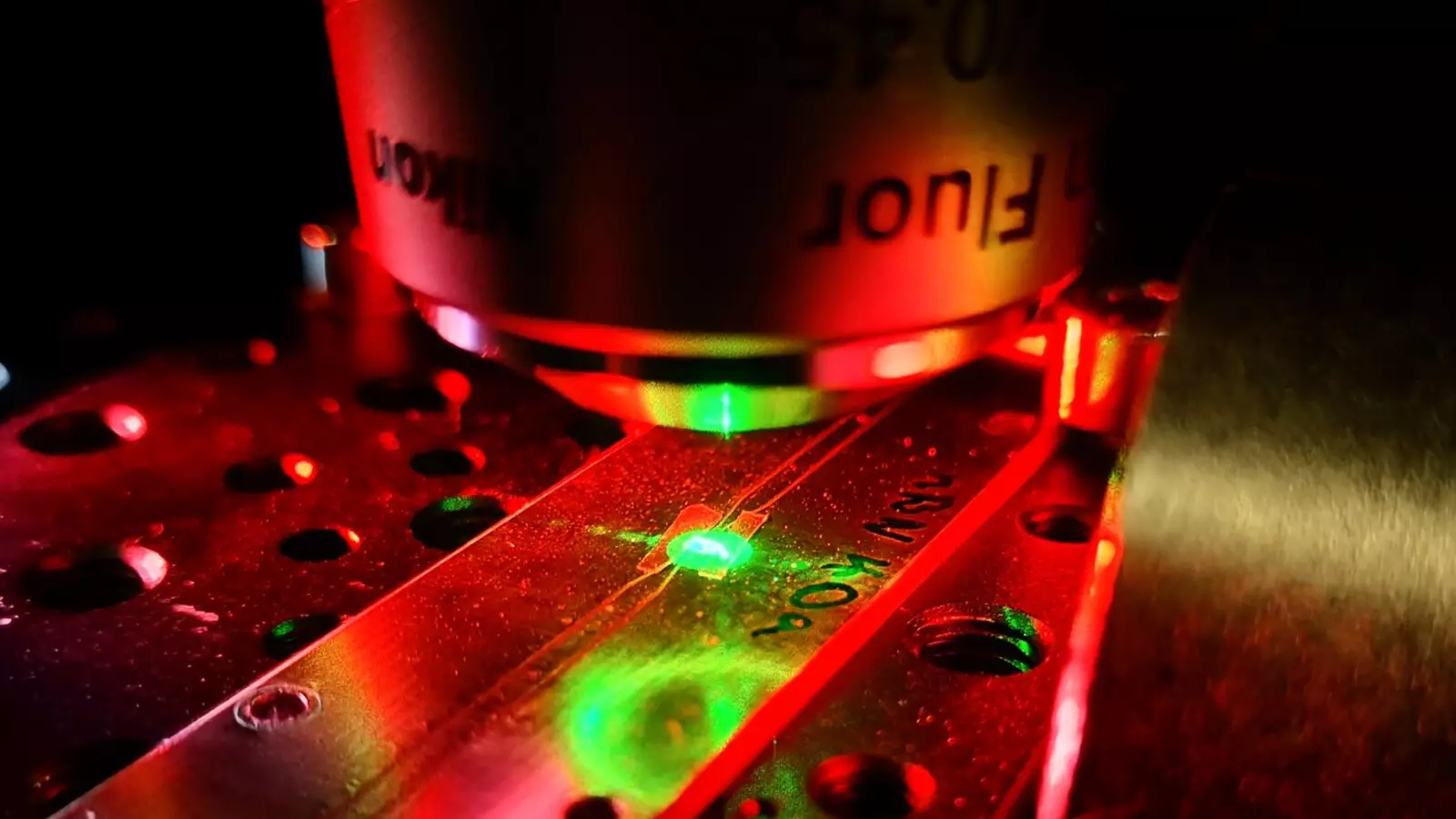
TMOS researchers, led by Associate Investigator Jean-Philippe Tetienne and Chief Investigator Igor Aharonovich, are at the forefront of pioneering a new quantum sensing platform using hBN crystals. The unique structure of hBN, consisting of atomically thin flexible layers, allows the sensor chips to conform to the shape of the sample being studied, enabling closer proximity than diamond sensors. The discovery of a carbon-based defect in hBN that behaves as a spin half system has unlocked the potential for detecting magnetic fields in any direction, marking a significant advancement in quantum sensing technology.
The optical spin defects in hBN offer a vital toolkit in the realm of quantum materials, allowing for nanoscale quantum sensors and robust room-temperature quantum systems. The 2D form of hBN provides a unique advantage, enabling sensors to approach samples much closer than previously possible. By harnessing the isotropic sensor capabilities of hBN, researchers have demonstrated the first magnetic images using this novel technology. The tunability and controllability of these sensors through electrical excitation present exciting prospects for future applications in various fields.
Compared to diamond, hBN offers several advantages as a quantum light source for communications and sensing. Its ultra-thin form factor, room-temperature operation, and cost-effectiveness make it a promising alternative to diamond, which often requires cryogenic cooling. The isotropic nature of hBN sensors opens up new possibilities for in-field identification of magnetic geological features and radio spectroscopy across a wider band, showcasing the vast potential of this new quantum sensing technology.
The next phase of research in this field involves identifying the atomic defects present in hBN to optimize sensor performance. By gaining a deeper understanding of these defects, researchers can tailor sensor devices for maximum efficiency and explore new opportunities in optical spin defect technology. The properties and opportunities offered by hBN sensors hold promise for advancing quantum sensing capabilities and unlocking new realms of physics in the realm of quantum materials.
Leave a Reply