Two-dimensional (2D) semiconducting materials offer unique optoelectronic properties that hold great promise for the advancement of ultra-thin and tunable electronic components. Despite their potential benefits compared to traditional bulk semiconductors, effectively integrating these materials with gate dielectrics has presented challenges, leading to interfacial traps that reduce transistor performance. However, researchers at King Abdullah University of Science and Technology (KAUST), Soochow University, and other institutions worldwide have recently introduced an innovative approach to overcome these challenges, potentially paving the way for the development of high-performance transistors based on 2D semiconductors.
The Proposed Design
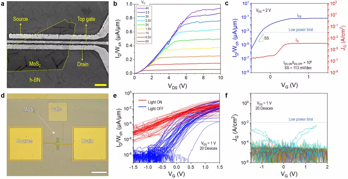
In a recent publication in Nature Electronics, researchers proposed a novel design utilizing hexagonal boron nitride (h-BN) dielectrics and metal gate electrodes with a high cohesive energy to enhance transistor performance. According to Yaqing Shen, the first author of the paper, initial experiments demonstrated that using platinum (Pt) as an anode reduced the likelihood of dielectric breakdown in the h-BN stack. Subsequent tests revealed that Pt/h-BN gate stacks exhibited significantly lower leakage currents than Au/h-BN gate stacks, along with a high dielectric strength of at least 25 MV/cm. These results inspired the researchers to explore the use of chemical vapor deposited h-BN as a gate dielectric in 2D transistors.
Transistor Fabrication Process
Shen, Prof. Mario Lanza, and their team fabricated over 1,000 devices using chemical vapor deposited h-BN as dielectrics. The fabrication process involved cleaning a SiO2/Si substrate, patterning Ti/Au source and drain electrodes using electron beam lithography, and transferring MoS2 onto these electrodes to create the channel. A CVD h-BN film was then transferred over the structure through a wet transfer method. In the final step, the researchers patterned the Pt gate electrode using electron beam lithography and deposited it using e-beam evaporation. The clean van der Waals interface between MoS2 and h-BN in the transistor design improved reliability and performance by minimizing defects and enhancing gate control.
Contrary to existing beliefs about the effectiveness of CVD h-BN as a gate dielectric, the study revealed that selecting the right metal electrodes, such as Pt and tungsten (W), enabled the utilization of CVD h-BN in field-effect transistors with MoS2 channels. The clean van der Waals interface between MoS2 and h-BN enhanced the reliability of the transistor, demonstrating the potential of high cohesive energy metals in maximizing the performance of 2D semiconductor-based devices. The research carried out by Shen and her team showcased a significant reduction in leakage currents and a high dielectric strength, setting the stage for the development of reliable solid-state microelectronic circuits and devices based on 2D materials.
The promising results of this research could inspire other research groups to explore similar approaches and materials, leading to the advancement of highly efficient 2D semiconductor-based devices. The development of ultra-small, fully 2D transistors could potentially contribute to extending Moore’s Law and driving further innovations in the field of microelectronics. As the research team looks ahead, the focus will be on developing nanoscale 2D transistors to push the boundaries of semiconductor technology and enable the realization of next-generation electronic devices.
Leave a Reply