In today’s digital landscape, the proliferation of artificial intelligence (AI) tools that analyze extensive datasets has unveiled a pressing need for advanced data storage technologies. As computations become increasingly complex, traditional memory solutions frequently fall short of what AI applications demand. This gap has prompted significant attention toward high-bandwidth memory technologies that promise rapid data transfer and reduced energy consumption. While conventional flash memory remains the dominant solution due to its non-volatile nature, it struggles with speed limitations that hinder optimal AI integration. As a result, researchers are focusing on the development of ultrafast flash memory devices capable of meeting these challenges.
Recent advancements in materials science have highlighted the potential of two-dimensional (2D) materials in revolutionizing memory technology. These materials, characterized by their exceptional electronic properties, provide unique avenues for creating faster and more efficient memory devices. Despite progress made with long-channel flash memory devices constructed from exfoliated 2D materials, scalability has remained a significant hurdle. The challenge lies in effectively integrating these components into functional memory arrays that can be reliably manufactured for widespread use.
In light of these challenges, a research team from Fudan University has made significant strides in addressing the scalability of ultrafast 2D flash memory devices. Their innovative approach, as discussed in their recent publication in *Nature Electronics*, successfully integrated 1,024 flash-memory devices, boasting a remarkable yield of over 98%. This research marks a critical step forward in overcoming the limitations previously posed by interface engineering issues that restricted the performance of 2D materials.
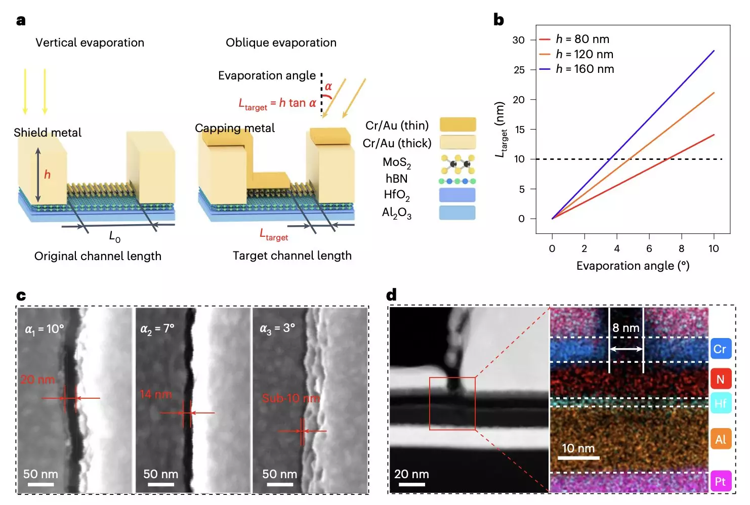
The researchers’ methodology involved utilizing a sophisticated combination of processing techniques, including lithography and e-beam evaporation, to fabricate their memory arrays. They demonstrated two distinct tunneling barrier configurations—HfO2/Pt/HfO2 and Al2O3/Pt/Al2O3—with the integration of monolayer molybdenum disulfide grown through chemical vapor deposition. Their experimental work illustrates the promising scalability of their invention, which allows for channel lengths to be reduced to sub-10 nanometers, significantly surpassing the conventional thresholds of silicon flash memory.
The innovations heralded by this research team provide compelling performance metrics: sub-10 nm devices not only maintain non-volatile storage capabilities but also deliver ultrafast speeds while holding up to four bits of information. Furthermore, the durability of these devices exceeds 100,000 write cycles, indicating their potential for long-term application in real-world settings. Key to the success of the researchers is their focus on achieving a high yield in fabrication, which is essential for commercial viability.
These advancements are crucial as the technology community seeks a way to bridge the existing gap between the rapid evolution of AI and the legacy challenges posed by traditional memory solutions. The implications of deploying such ultrafast flash memory devices extend beyond mere efficiency; they may redefine how data is processed, especially in high-demand environments like machine learning and big data analytics.
As promising as these advancements are, further exploration is necessary to realize the full potential of 2D materials for data storage applications. Future research efforts could focus on integrating flash memory arrays utilizing various 2D materials and configurations to achieve even greater performance enhancements. Innovations in memory architecture will play a significant role in overcoming the remaining challenges of scalability and yield.
In essence, the journey toward realizing ultrafast flash memory technologies embodies the dynamic interplay between materials science, engineering, and computing demands. The work done by the Fudan University team not only demonstrates the possibilities inherent in this field but also sets the foundation for an evolving landscape of data storage solutions tailored to meet the exigencies of tomorrow’s computational needs.
The quest for ultrafast flash memory solutions symbolizes a critical phase in the ongoing evolution of data storage technology. With 2D materials paving the way for improved performance and efficiency, the potential for commercial applications is expanding rapidly. As researchers continue to refine their approaches and explore new configurations, the prospect of a future where data storage can seamlessly keep pace with AI advancements becomes increasingly attainable. The innovations emerging from this research not only represent significant technological progress but also signal a transformative shift in how we approach memory storage in the age of artificial intelligence.
Leave a Reply