The quest for materials that can enhance electronics performance beyond the limitations of silicon-based transistors has led researchers to explore two-dimensional (2D) semiconductors. With atomically thin structures and high carrier mobilities, 2D semiconductors hold great promise for improving the electrostatic control and ON-state performances of short-channel field-effect transistors (FETs).
Despite their advantages, 2D semiconductors face a significant challenge in the form of high contact resistances due to Fermi-level-pinning effects. These effects have hindered the effective integration of 2D semiconductors in electronics, limiting their potential for large-scale fabrication.
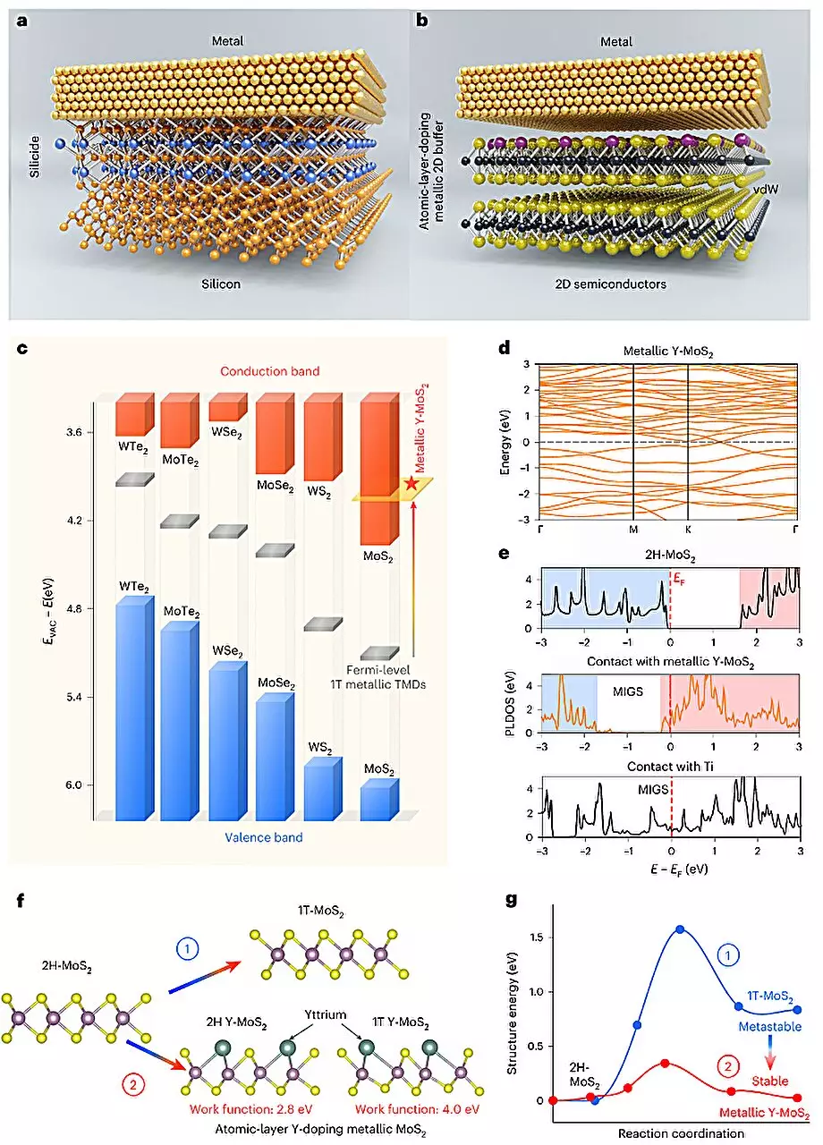
A recent study by researchers at Peking University and Chinese Academy of Sciences introduced a novel yttrium-doping strategy to address the issue of Fermi-level pinning effects in 2D semiconductors. By converting semiconducting molybdenum disulfide (MoS2) into metallic MoS2, the researchers were able to improve band alignment and enable the use of MoS2 for fabricating ohmic contacts in 2D transistors.
The researchers developed a plasma-deposition-annealing (PDA) method for yttrium doping in the surface layer of MoS2. This process involved treating patterned local contact areas with low-power soft plasma to create active sites, followed by the deposition of a Y/Ti/Au stacked metal with a 1 nm-thick active metal Y as a solid-state doping source. The Y atoms diffused into the active sites and were activated in the top layer of the material through high-temperature annealing in an inert gas environment.
The researchers introduced a new concept in their paper, known as “rare earth element yttrium doping-induced 2D phase transition.” This phase transition led to the metallization of MoS2 when the yttrium doping strategy was applied. By developing a selective-area single-atomic-layer surface doping technique, the researchers were able to achieve a doping depth as low as 0.5 nanometers, pushing the limits of traditional ion implantation doping.
The application of the yttrium-doping strategy resulted in the development of ultra-short MoS2-based channel ballistic transistors with excellent performance as ohmic contacts and impressive switching capabilities. These transistors hold the potential to contribute to the creation of new sub-1 nanometer node chips that deliver remarkable performance while consuming less power compared to conventional chips.
Looking ahead, the researchers aim to develop equally high-quality p-type ohmic contacts suitable for 2D semiconductors, further advancing the field of electronics. By overcoming the limitations of traditional doping techniques and harnessing the unique properties of 2D semiconductors, the potential for innovation in transistor design and fabrication continues to grow.
The integration of yttrium doping in 2D semiconductors represents a significant advancement in the field of electronics, offering a pathway to enhanced transistor performance and the development of next-generation semiconductor devices. As researchers continue to explore novel materials and techniques, the future of electronics looks promising with the potential for smaller, more powerful, and energy-efficient devices on the horizon.
Leave a Reply