Antiferromagnetic materials represent a fascinating area of study within condensed matter physics, characterized by their unique property of exhibiting no net macroscopic magnetism. This occurs due to the antiparallel alignment of magnetic moments among neighboring atoms, leading to an intriguing interplay of magnetic interactions. As researchers delve deeper into these materials, there is growing interest in their potential applications in spintronic and electronic technologies. The recent discoveries at Harvard University signify a substantial step in harnessing these properties to create groundbreaking devices that could innovate the field.
The researchers at Harvard focused on even-layered manganese-bismuth telluride (MnBi2Te4), an antiferromagnetic topological insulator. This material stands out due to its centrosymmetric structure which, surprisingly, enables the observation of the antiferromagnetic diode effect despite the lack of directional charge separation. The significance of this finding cannot be understated, as it challenges existing notions about the conditions required to produce diode effects in materials and opens new avenues for device applications.
Historically, diode effects have been confined to materials with directional charge transport properties, which are fundamental to the operation of numerous electronic devices, including radio receivers and digital circuits. The Harvard team’s findings suggest that even structures devoid of traditional symmetry principles can facilitate similar functionalities, potentially leading to a paradigm shift in device design.
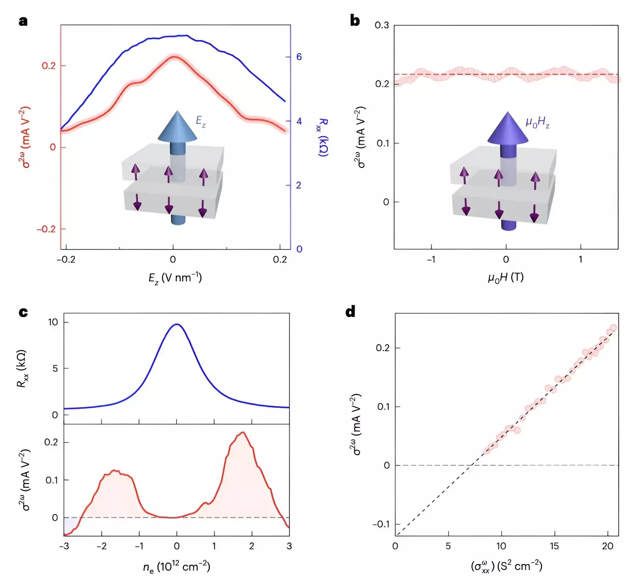
To validate their hypotheses, the researchers employed a range of advanced techniques, including spatially resolved optical methods and electrical sum frequency generation (SFG) measurements. These methods proved crucial in providing detailed insights into the nonlinear transport phenomena exhibited by the MnBi2Te4 devices. The novelty of their approach lies not only in the material used but also in the diversity of electrode configurations, such as Hall bar electrodes and radially distributed electrodes, which further broaden the experimental landscape.
The combination of these innovative designs and measurement strategies allowed the team to obtain robust evidence supporting their claim of an antiferromagnetic diode effect. Observations of significant second-harmonic transport underscore the material’s uniqueness and its potential role in creating specialized electronic architectures.
The implications of the observed antiferromagnetic diode effect are profound. As the authors suggest, this groundbreaking research paves the way for developing in-plane field effect transistors and efficient microwave energy harvesting devices. These applications highlight the shift towards integrating antiferromagnetic materials into mainstream electronic infrastructures, facilitating faster, more reliable devices while potentially reducing energy consumption.
Moreover, the introduction of antiferromagnetic logic circuits presents an exciting frontier in computational technologies. Unlike traditional semiconductor logic, antiferromagnetic circuits could leverage spin-based operations, promising enhanced speed and reduced heat output. With the ability to harness quantum and nonlinear effects wisely, the researchers at Harvard could spark new interest in fundamental studies aimed at pushing the boundaries of current technology.
The observations made by the Harvard research team invite researchers across disciplines to explore the vast landscape of antiferromagnetic materials. Their findings encourage further investigation into the underlying principles of the antiferromagnetic diode effect and its applicability in emerging technologies. The response to electrical signals in antiferromagnetic compounds may hold solutions to some of the most pressing challenges in modern electronics, including those related to power efficiency and operational speed.
As these avenues of research evolve, the continued collaboration among physicists, materials scientists, and engineers will be vital for translating these discoveries from academic studies into commercially viable technologies. With the promise of antiferromagnetic materials and their unique properties now under the spotlight, we are likely to witness a renaissance in the development of innovative devices that could redefine the electronics and spintronics fields.
The Harvard University team’s pioneering work shifting perceptions around antiferromagnetic materials paves the way for future technological innovations. As these materials find their place on the technological landscape, we stand on the brink of a new era marked by sophisticated devices that harness the power of spintronics for the digital age.


Leave a Reply